Building an ADC on a Keychain
Published on
Table of Contents
A few times recently, I’ve found myself wanting a memorable business card to give out. Being an electrical engineer, I figured I’d have some fun and build a cool fidget circuit onto a PCB small enough to hand out at meetings. I decided to build a little ADC (analog-to-digital converter) demo from scratch, because who doesn’t like an ADC fidget toy?
The Idea Link to this section
The idea was to included a dummy analog input ‘signal’, a scratch-built ADC, and an LED output to show a digital readout of the analog voltage. This should be small enough to fit on a card, without being so small that people can’t inspect and play with the components themselves. Most importantly, it should be fun to fidget with, and ideally a conversation starter.
For the ADC, I figured a residue amplifier ADC would be fun and lend itself to a more interesting circuit layout… this is after all a showcase piece. Residue amplifier ADCs don’t get much attention these days, but they have their niche. For the electrical engineers in the audience: a residue amplifier ADC lies somewhere in the tradeoff space between a flash ADC and an SAR ADC. Not quite as fast as a flash ADC, but much smaller and still much faster than a SAR.
ADC Design Link to this section
A residue amplifier ADC is constructed from a chain of… wait for it… residue amplifiers. A residue amplifier is an analog circuit which computes the digital division of the input signal, and outputs an analog remainder (or residue) after the division. I’ve drawn an example using opamps:
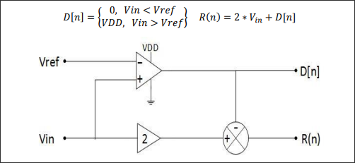
Essentially, D[n] outputs logic high if Vin > Vref, and R(n) is the
amplified remainder. In essence, this is a 1-bit digital division of Vin / Vref. 1-bit is not very interesting by itself, but the magic happens when you
chain them together, and successively perform a 1-bit division on the
remainder, you end up computing an n-bit division. Note, this is not
necessarily a base-2 bit. The base is the ratio of VDD / Vref. To get a
traditional binary output, I set Vref == 1/2 VDD. From here, I can chain a
few of these together to to get the n-bit digital conversion of the analog
signal 🎉.
To help illustrate this, I mocked up a chain of 2 residue amplifiers for a simple 2-bit ADC, and plot their intermediate signals:
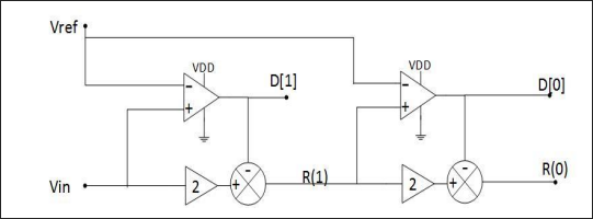
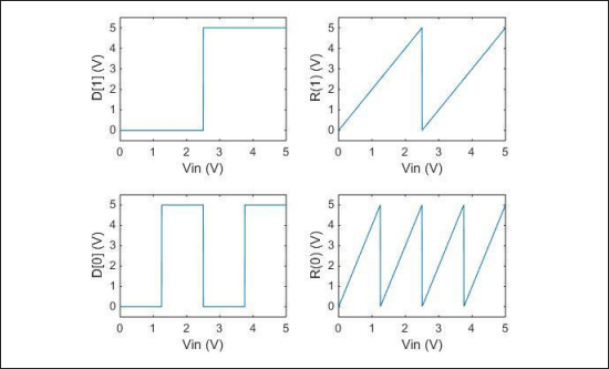
This gives some insight into how each digital value is calculated from the
residue of the previous. One detail I have glossed over until now, is the fact
that we amplify the residue by a factor of 2. This is because we are comparing
against 1/2 VDD, so the residue is range-bound to <1/2 VDD. To bring the
residue back to full-scale, we multiply by 2.
PCB Design Link to this section
Now, to build my keychain, I’ve decided to build a 4-bit
version of the aforementioned design. I’ll also use a
low-profile potentiometer to provide a nice fidgety input
signal (user can twist to sweep input from 0 to VDD), and an
LED output at each D[n] for a visual readout:
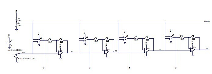
Using a total of 8 opamps, I can achieve a compact layout using two quad-amp ICs:
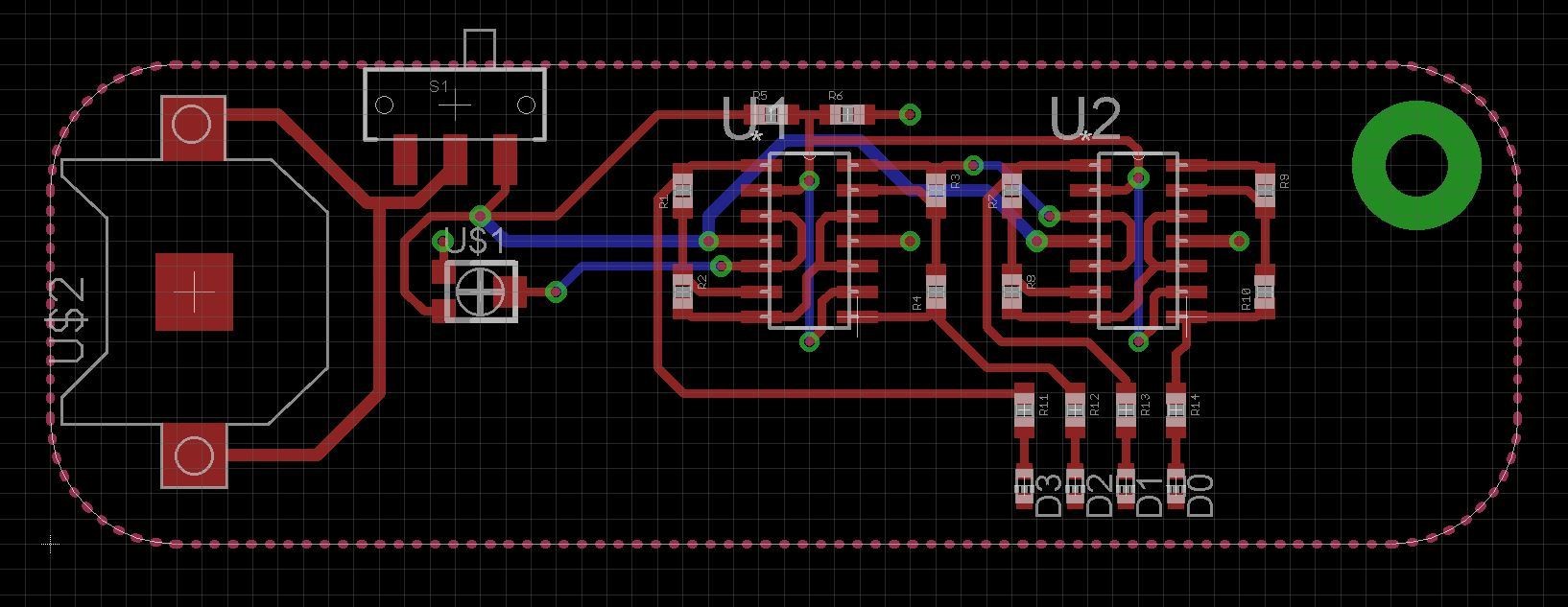
Here is the BOM I selected:
| Qty | Description | Part number |
|---|---|---|
| 2 | TLV274IDR | Quad Operational Amplifier. Mouser p/n: 595-TLV274IDR |
| 2 | 10 KOhm - 0603 SMD resistors | Mouser p/n: 71-CRCW0603-10K-E3 |
| 8 | 1 KOhm - 0603 SMD resistors | Mouser p/n: 71-CRCW0603-1.0K-E3 |
| 4 | 100 Ohm - 0603 SMD resistors | Mouser p/n: 71-CRCW0603-100-E3 |
| 4 | LNJ826W86RA | LEDs: Mouser p/n: 667-LNJ826W86RA |
| 1 | 10 K potentiometer | Mouser p/n: 652-TC33X-2-503E |
| 1 | SMD Switch | Mouser p/n: 611-AYZ0102AGRLC |
| 1 | CR 1225 Battery Holder | Mouser p/n: 614-SMTM1225 |
| 1 | CR 1225 Battery | Mouser p/n: 614-CR1225.IB |
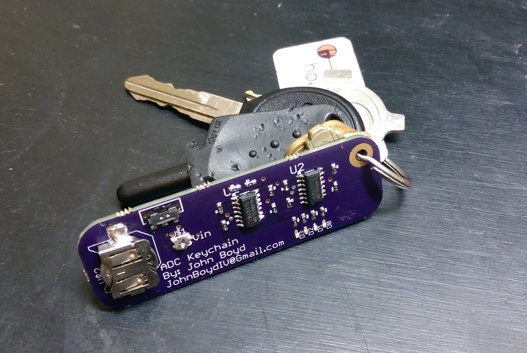
After a quick-turn PCB run, here’s the finished gadget:
The finished result. A fun, fidgety, ADC keychain.
Conclusion Link to this section
This is one of those projects that has no real technical purpose, but it was fun. I’m happy to say this piece has started many conversations, albeit with a very niche crowd 🤓.
For anyone who is interested, you can find the design files on Github.
